Basic Verilog
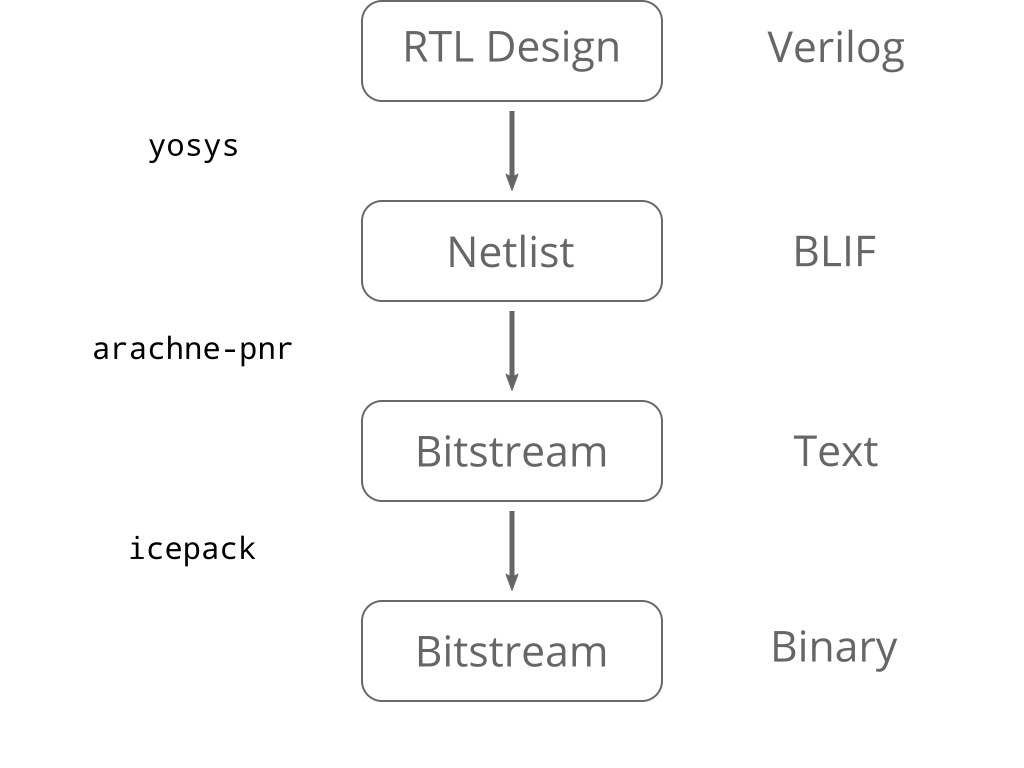
The Process

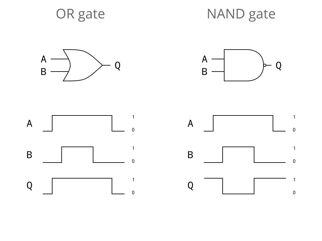
Combinatorial Logic

Sequential Logic

Register Transfer Logic
Designing individual gates and flip-flops is possible, but infeasible on huge modern chips. Instead:
- we group flip flops together into registers to hold the state of one or more bits.
- we connect registers by networks of wires, or nets.
We will use Verilog to describe this. It provides
- modules to structure our design
- sequential logic to control how state moves between registers on clock edges
- combinatorial logic to link together nets continuously.
The LED Example: led.v
This continuously assigns the value 1 to the LED pin:
module led (output led);

   assign led = 1;

endmodule
But how does this understand that led is connected to the LED?
Interface to the LED Example: chip.v (1)
The module declaration tells us about all our input and output signals:
module chip (
    // 100MHz clock input
    input  clk,
    // SRAM Memory lines
    output [18:0] ADR,
    output [15:0] DAT,
    output RAMOE,
    output RAMWE,
    output RAMCS,
    // All PMOD outputs
    output [55:0] PMOD,
    input [1:0] BUT
  );
Interface to the LED Example: chip.v (2)
We can use continuous assignment to set signals we don’t want to use:
// SRAM signals are not use in this design, lets set them to default values
assign ADR[18:0] = {19{1'b0}};
assign DAT[15:0] = {16{1'b0}};
assign RAMOE = 1'b1;
assign RAMWE = 1'b1;
assign RAMCS = 1'b1;

// Set unused pmod pins to default
assign UART_TX = PMOD[11];
assign PMOD[54:12] = {42{1'b0}};
assign PMOD[10:00] = {11{1'b0}};
Interface to the LED Example: chip.v (3)
And finally we instantiate an instance of the led module inside the
chip module.
  led my_led (
    .led (PMOD[55])
  );

endmodule
PMOD[55] is the external pin corresponding to the red LED. But how does
Verilog know that?
The Physical Constraints File (1)
The file blackice.pcf maps the named top level ports to actual pin
numbers on the FPGA:
#pmod 1
set_io PMOD[0] 94 # rd6
set_io PMOD[1] 91 # rd4
set_io PMOD[2] 88 # rd2
set_io PMOD[3] 85 # rd0
...
#pmod 14 SPI muxed with leds
set_io PMOD[52] 71 #LD4,!SS,p14_1
set_io PMOD[53] 67 #LD3,MISO,p14_2
set_io PMOD[54] 68 #LD2,MOSI,p14_3
set_io PMOD[55] 70 #LD1,SCL,p14_4
The Physical Constraints File (2)
# SRAM
set_io ADR[0] 137
set_io ADR[1] 138
set_io ADR[2] 139
...
# Onboard 12Mhz oscillator
set_io clk 129

# Buttons
set_io BUT[0] 63
set_io BUT[1] 64
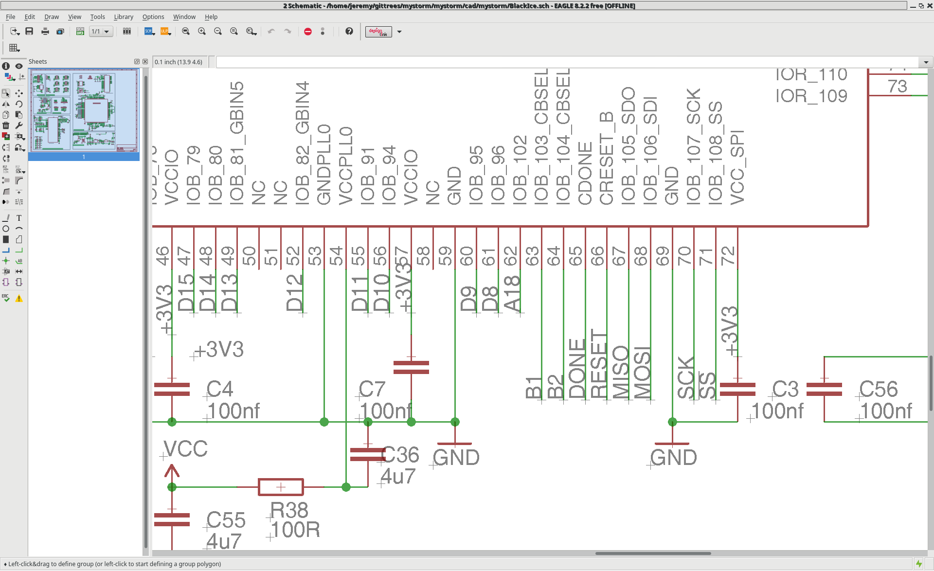
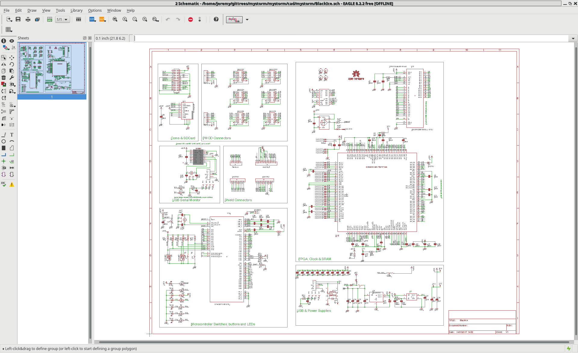
But where do you find the pin numbers?
MyStorm Schematic Detail

Exercise 1
Start with led.v in the basic_verilog/led directory. Complete it and
build it with:
make led
Then try the following changes:
- Modify
led.vandchip.vto light one of the other LEDs. - Try lighting up more than one LED at once.
Next stage of the tutorial, we’ll get the LED to change depending on which button is pressed.
